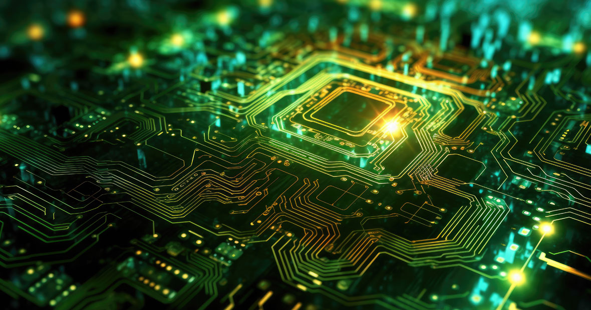
High-Density Interconnect (HDI) Printed Circuit Boards (PCBs) have become a necessity in the world of high-speed and high-frequency electronic devices. Leveraging the potential of these advanced boards, engineers and designers are addressing common challenges in electronic design, such as signal integrity, material selection, and routing. This discourse examines the use of HDI PCBs in high-speed electronic design, the implications of material selection for these applications, and recent innovations in PCB layer stack-up that enhance performance. The mounting difficulties in routing and maintaining signal integrity in high-speed design will be another focal point of discussion. Furthermore, the narrative delves into the effects of HDI PCBs on signal integrity and transmission quality, alongside a look at groundbreaking manufacturing techniques tailored for these circuit boards in high-speed devices. The utilization of microvias for compact circuit design, implementation of rigid-flex technologies for dynamic applications, and the role of quality control in HDI PCB fabrication will all be scrutinized in the following sections.
Exploring hdi pcbs in high-speed electronic design
Modern electronics are seeing a paradigm shift towards compact, high-performance gadgets. HDI PCBs, or High-Density Interconnect Printed Circuit Boards, have been a cornerstone of this revolution. By providing a solution for high-speed signal management, they significantly elevate the overall performance of electronic devices. It is their exceptional ability to reduce latency in high-speed data communication systems that makes them an integral component of modern electronics.
Choosing the Right Materials for High-Speed Applications
The utilization of HDI PCBs in devices requiring precision and reliability hinges on the selection of materials. Given the demand for higher performance and miniaturization, the choice of materials has a profound impact on the design and functionality of HDI PCBs.
Innovations in PCB Layer Stack-Up for Enhanced Performance
Layer stack-up has seen significant innovations in HDI PCBs, leading to enhanced performance. With an increase in the number of layers, PCBs can accommodate more components, thus supporting the shift towards more compact, powerful devices.
Challenges in Routing and Signal Integrity in High-Speed Design
As the complexity of electronic design increases, so do challenges in routing and signal integrity. Ensuring optimal performance of high-speed devices requires innovative solutions from the industry, particularly from HDI PCB manufacturers. High-speed design, therefore, relies on the ongoing advancements within the industry.
Looking ahead, the future of HDI PCB design points towards further integration and improved data transmission capabilities, promising a new era in electronic design.
Material considerations for high-frequency hdi pcb applications
Understanding the material considerations for high-frequency HDI PCB applications is paramount. In the world of high-speed applications, the choice of materials with low dielectric properties plays a crucial role in optimizing the performance of these applications. Advanced composite materials are being evaluated for their superior heat and mechanical resistance. These materials enhance the signal speed and noise reduction in high-frequency applications, thereby improving the overall performance of HDI PCBs.
Another significant factor is the thermal expansion rate of the materials used. Materials with low thermal expansion provide reliability and stability to the connections in high-frequency environments. Moreover, these materials have a positive impact on the miniaturization of components and the densification of HDI PCBs. Not to forget, the constant performance of high-frequency HDI PCB applications is ensured by considering the moisture absorption properties of the materials. Therefore, understanding these aspects is essential for efficient and effective high-frequency HDI PCB applications.
Impact of hdi pcbs on signal integrity and transmission quality
Signal integrity assumes a pivotal position in the performance of high density interconnect (HDI) printed circuit boards (PCBs). With an increasing demand for smaller, faster technology, HDI PCBs have taken the spotlight for their ability to maintain signal integrity, even in high-frequency applications.
HDI PCBs have been observed to effectively minimize signal loss, thus enhancing transmission quality. This is primarily due to the strategic layout of layers, which manifests in improved signal integrity. A significant factor in this performance is the management of impedance, a component that, when properly controlled, can significantly uplift transmission quality.
Further, the use of buried and blind vias has a marked effect on the transmission performance of HDI PCBs. These vias reduce crosstalk, a phenomenon that could otherwise compromise the integrity of signals. Moreover, the surface contact area and component density also play a vital role in optimizing the performance of HDI PCBs.
In the realm of high-speed and high-frequency applications, the impact of these factors in HDI PCBs cannot be understated. The ability to reduce signal loss, manage impedance, and reduce crosstalk makes HDI PCBs an important asset in the electronics industry.
Advanced manufacturing techniques for hdi pcbs in high-speed devices
Unprecedented strides are seen in the realm of electronics, with a primary focus on high density interconnect (HDI) printed circuit boards (PCBs). These HDI PCBs, known for their use in high-speed and high-frequency applications, incorporate advanced manufacturing techniques that significantly enhance their performance.
Utilizing Microvias for Compact and Efficient Circuit Design
Central to the success of HDI PCBs in high-speed devices is the involvement of microvia techniques. These enable a high connection density, yielding compact and efficient circuit designs. The application of advanced materials complements these techniques, amplifying the thermal and electrical performance of the PCBs. Complex circuit routing strategies are employed to optimize signal integrity, critical in high-speed applications.
Implementing Rigid-Flex Technologies for Dynamic Applications
Innovation further continues with the introduction of rigid-flex technologies in the assembly process. This approach is utilized for the assembly of components on rigid-flex PCBs, fostering more compact configurations. The integration of optimized power and ground layers aids in effective power management in electronic devices.
Quality Control and Testing in HDI PCB Fabrication
The final stage of the manufacturing process involves stringent quality control measures and testing. Advanced testing capabilities are integrated during the fabrication process. This ensures both reliability and high performance in high-frequency applications, with a distinct emphasis on trace routing, circuit layers and thermal management.